Need more?
| Quantity | Price |
|---|---|
| 1+ | $22.660 |
| 10+ | $18.110 |
| 25+ | $17.200 |
| 50+ | $16.290 |
| 100+ | $15.720 |
| 250+ | $15.130 |
| 500+ | $14.770 |
Product Information
Product Overview
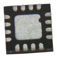
ADCLK914 is an ultrafast clock/data buffer fabricated on the Analog Devices, Inc., proprietary, complementary bipolar (XFCB-3) silicon-germanium (SiGe) process. It features high voltage differential signaling (HVDS) outputs suitable for driving the latest Analog Devices high speed digital to-analog converters (DACs). It has a single, differential open-collector output. The input has a center tapped, 100 ohm, on-chip termination resistor and accepts LVPECL, CML, CMOS, LVTTL, or LVDS (ac-coupled only). A VREF pin is available for biasing ac-coupled inputs. It is widely used in application such as clock and data signal restoration, high speed converter clocking, broadband communications, cellular infrastructure, high speed line receivers, ATE and high performance instrumentation, level shifting, threshold detection etc.
- Operating frequency is 7.5GHz typical
- Propagation delay is 158ps typical
- Output rise time is 100ps typical
- Wideband random jitter is 110fs rms typical
- On-chip input terminations
- 3.3V power supply (VCC − VEE)
- Input bias current is 20µA typical
- Supply voltage range is 2.97V to 3.63V
- Operating temperature is -40°C to +125°C
- Package style is 16-lead lead frame chip scale package [LFCSP]
Notes
ADI products are only authorized (and sold) for use by the customer and are not to be resold or otherwise passed on to any third party
Technical Specifications
Clock Buffer
7.5GHz
1Outputs
3.63V
16Pins
-
125°C
No SVHC (04-Feb-2026)
7.5GHz
LFCSP-EP
2.97V
LFCSP-EP
-
-40°C
MSL 3 - 168 hours
Technical Docs (1)
Legislation and Environmental
RoHS
RoHS
Product Compliance Certificate
